
This time we will focus on modern Graphics Processing Units (GPU) through the generations, AMD Edition.
Radeon Through the GenerationsThe modern GPU that we are familiar with today and the only kind of GPU that AMD, Intel, or Nvidia makes today is the kind with a Unified Shader architecture. A shader is how the computer calculates the lighting and color of an object simulated in a 3D scene. Before the unified shader paradigm, graphics cards would have separate dedicated hardware for each of the multiple steps of processing. The first step is Vertex Shading, calculating the lighting and color of the model of the object itself, the second step is the pixel shader where the color of each pixel on the computer's display is calculated. A Unified shader is a processor that is capable of calculating both of these steps rather than only just one.
2007 - TeraScale TwiceATI initially developed the Unified Shader for the Xbox 360 in 2006, but did not manage to fit it into a Desktop GPU until the HD 2900 XT was released in May of 2007 for $399. The new architecture used to usher in this new era of GPUs was called TeraScale. Features included the Unified Shader model and support for DirectX 10. In November 2007, the next generation HD 3870 was released for $269. It was a slightly refined version that was built smaller and more efficient in order to lower the price and target a lower performance market segment. ATI made the switch to PCI-E 2.0 and added support for DirectX 10.1 with this card.
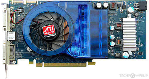
| Model | Codename | Architecture | Transistor Count | Video Memory | PCI-E Interface | TDP | Passmark Score |
| HD 2900 XT | R600 XT | 80nm TeraScale 1.0 | 720 Million | 512MB GDDR3 | PCI-E 1.0 | 215 Watts | 659 |
| HD 3870 | R670 XT | 55nm TeraScale 1.0 | 666 Million | 1GB GDDR3 | PCI-E 2.0 | 106 Watts | 547 |
The HD 4870 was released in June 2008 for $299. It was still using the same TeraScale 1.0 architecture, but it now used the much faster GDDR5 memory. Full hardware H.264 encoding was also introduced in these cards. This was the first card developed completely by AMD, but it was still released under the ATI brand name.
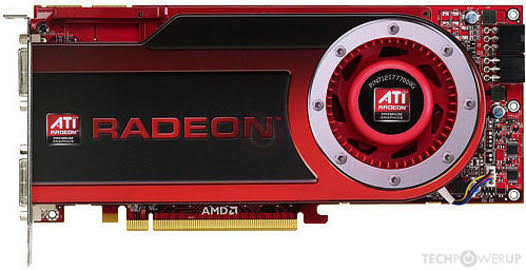
| Model | Codename | Architecture | Transistor Count | Video Memory | PCI-E Interface | TDP | Passmark Score |
| HD 4870 | RV770 XT | 55nm TeraScale 1.0 | 956 Million | 2GB GDDR5 | PCI-E 2.0 | 150 Watts | 719 |
The HD 5870 was released in September 2009 for $379 and it brought a more refined version of the TeraScale 1.0 architecture called TeraScale 2. AMD (still using the ATI brand name) made TeraScale 2 a little bit bigger and better in every way. This included a bigger processor, more power, support for DirectX 11, PCI-E 2.1, and the introduction of the Eyefinity multi-monitor support, which allowed users to combine multiple monitors into a single virtual monitor in the driver software.
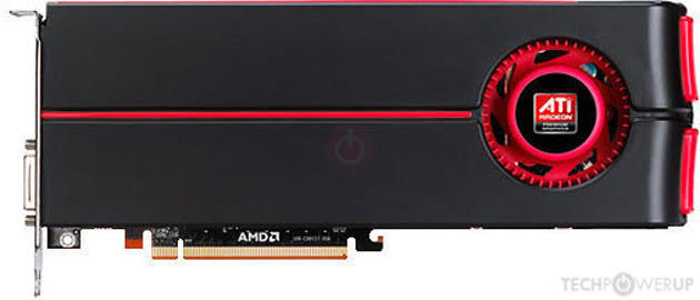
| Model | Codename | Architecture | Transistor Count | Video Memory | PCI-E Interface | TDP | Passmark Score |
| HD 5870 | Cypress XT | 40nm TeraScale 2.0 | 2.15 Billion | 2 GB GDDR5 | PCI-E 2.1 | 188 Watts | 1153 |
2010 is when AMD decided to retire the ATI brand name and released the AMD Radeon HD 6970 in December 2010 for $369 under its own brand. This year also brought a newly refined TeraScale architecture called TeraScale 3. TeraScale 3 introduced dynamic frequency scaling that helped lower idle power usage as well as prevent overheating.
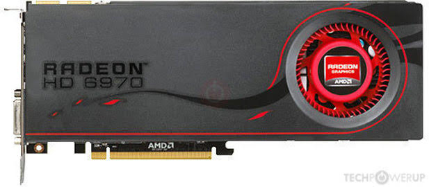
| Model | Codename | Architecture | Transistor Count | Video Memory | PCI-E Interface | TDP | Passmark Score |
| HD 6970 | Cayman XT | 40nm TeraScale 3.0 | 2.64 Billion | 2 GB GDDR5 | PCI-E 2.1 | 250 Watts | 3102 |
2012 brought about a brand new GPU architecture called Graphics Core Next, or GCN 1.0. The HD 7970 was released in January 2012 for $549. GCN was fast and it supported DirectX 12. It was also when AMD made the upgrade to PCI-E 3.0. This architecture was chosen to power the graphics of the Xbox One released in 2013.
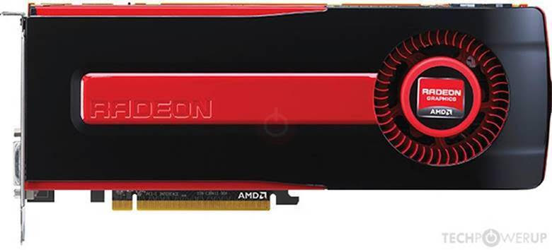
| Model | Codename | Architecture | Transistor Count | Video Memory | PCI-E Interface | TDP | Passmark Score |
| HD 7970 | Tahiti XT | 28nm GCN 1.0 | 4.3 Billion | 3GB GDDR5 | PCI-E 3.0 | 250 Watts | 5247 |
AMD refined GCN 1.0 into a very hot and power hungry version called GCN 2.0 and released the R9 290X in November 2013 for $549. GCN 2.0 introduced new features such as Variable Refresh Rate, which went unused until the release of FreeSync in 2015, and Virtual Super Resolution, which rendered a scene above the native resolution and then downsampled it for better image quality. Previously this was done in the game itself, but now could be done by the GPU driver. AMD also introduced True Audio, a 3D audio engine that was abandoned soon after. GCN 2.0 is also when the Mantle API support was introduced. Mantle was donated to the Khronos Group where they used it to develop the now popular Vulkan API, a worthy competitor to the most advanced features of DirectX 12. GCN 2.0 was the architecture chosen to be used in the PS4 released later this year.
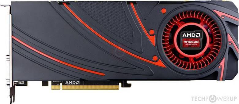
| Model | Codename | Architecture | Transistor Count | Video Memory | PCI-E Interface | TDP | Passmark Score |
| R9 290X | Hawaii XT | 28nm GCN 2.0 | 6.2 Billion | 4GB GDDR5 | PCI-E 3.0 | 290 Watts | 8011 |
In June 2015 AMD released the R9 390X for $429. Even though it was really just an R9 290X with more memory so the only noticeable difference was better performance at higher resolutions. The real star of 2015 was the R9 Fury X that also launched in June 2015 for $649. The R9 Fury X was so big, and so hot that it required an included water cooler out of the box. GCN 3.0 was a further refinement of the GCN platform with numerous improvements to features such as color compression, video encoding, tessellation performance. The biggest new feature of the R9 Fury X was the inclusion of the brand new and very fast High Bandwidth Memory (HBM) for the VRAM. HBM uses stacked DRAM modules meaning that they can all be kept very close together and placed very close to the GPU itself, allowing for extremely high speeds and throughput. The Radeon Fury X marked the first time that the high-end flagship card from AMD was named completely differently from the rest of the cards from AMD. AMD would continue this tradition in later years.
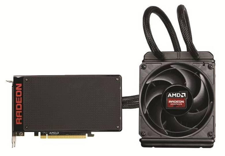
| Model | Codename | Architecture | Transistor Count | Video Memory | PCI-E Interface | TDP | Passmark Score |
| R9 390X | Hawaii XT | 28nm GCN 2.0 | 6.2 Billion | 8GB GDDR5 | PCI-E 3.0 | 275 Watts | 8011 |
| R9 Fury X | Fiji XT | 28nm GCN 3.0 | 8.9 Billion | 4GB HBM | PCI-E 3.0 | 275 Watts | 9988 |
GCN 4.0 was refined to be smaller in every way. Smaller process node, smaller GPU, smaller power draw, lower heat, and much smaller price. The RX 480 released in June 2016 for $199. These refinements were mostly efficiency based and added support for HDR10.
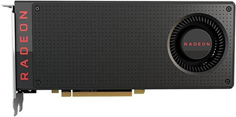
| Model | Codename | Architecture | Transistor Count | Video Memory | PCI-E Interface | TDP | Passmark Score |
| RX 480 | Polaris 10 | 14nm GCN 4.0 | 5.7 Billion | 8GB GDDR5 | PCI-E 3.0 | 150 Watts | 8471 |
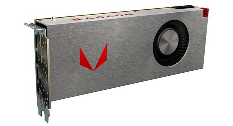
In 2017 AMD continued the new tradition of naming the new Flagship something completely different from the mid-range, more affordable options. The Radeon RX 580 was released in April 2017 for $199. This was basically an RX 480 with slight improvements to power and heat management in order to reach higher clock speeds. The real flagship was the Radeon RX Vega 64, released in August 2017 for $499. This GPU used the newly refined GCN 5.0. The refinements of GCN 5.0 included moving back to HBM with the new HBM2 memory along with numerous improvements to the processor itself such as more flexible compute units and improvements to the shader processing making the card much faster.
| Model | Codename | Architecture | Transistor Count | Video Memory | PCI-E Interface | TDP | Passmark Score |
| RX 580 | Polaris 20 | 14nm GCN 4.0 | 5.7 Billion | 8GB GDDR5 | PCI-E 3.0 | 185 Watts | 8712 |
| RX Vega 64 | Vega 10 | 14nm GCN 5.0 | 12.5 Billion | 8GB HBM2 | PCI-E 3.0 | 295 Watts | 15005 |
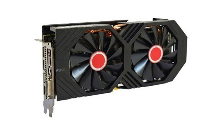
The RX 590 released November 2018 for $279. It wasn't so much a further refinement of GCN as it was the same GCN 4.0 made using a more modern process. The modern process allowed it to reach higher clocks at cooler temperatures so it was sold as a new, faster GPU. AMD didn't even bother releasing their own design and only left it up to third party manufacturers to come up with the designs.
| Model | Codename | Architecture | Transistor Count | Video Memory | PCI-E Interface | TDP | Passmark Score |
| RX 590 | Polaris 30 | 12nm GCN 4.0 | 5.7 Billion | 8GB GDDR5 | PCI-E 3.0 | 225 Watts | 9512 |
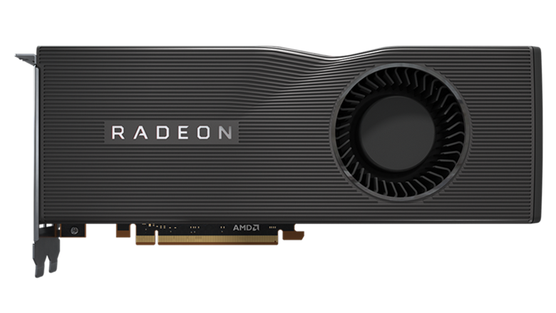
AMD released another odd-named flagship called the Radeon VII in February 2019 for $699. The Radeon VII used a more modern process to manufacture the same GCN 5.0 from 2017. But, the smaller modern process node allowed it to run much, much more efficiently, allowing even higher clock speeds at a lower power usage. But, that didn't stop AMD from cranking up the power in order to make it even faster. A newly refined memory controller featured lower memory latency and support for the new GDDR6 memory. All this put together made one seriously powerful graphics card. AMD also changed up the naming scheme for the lower tier GPUs this year to signify the release of a brand new architecture named Radeon DNA (RDNA) featuring a mix of refined GCN parts along with some brand-new designed parts. The Radeon RX 5700 XT was released July 2019 for $399.
| Model | Codename | Architecture | Transistor Count | Video Memory | PCI-E Interface | TDP | Passmark Score |
| Radeon VII | Vega 20 | 7nm GCN 5.0 | 13.2 Billion | 16 GB HBM2 | PCI-E 3.0 | 300 Watts | 17133 |
| RX 5700 XT | Navi 10 | 7nm RDNA 1.0 | 10.3 Billion | 8GB GDDR6 | PCI-E 3.0 | 225 Watts | 16587 |
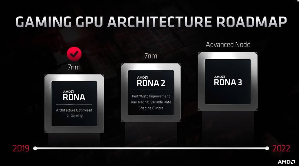
RDNA 2.0 arrived in 2020, and it was a big deal for a couple of reasons. Most importantly, it was AMD's first architecture with dedicated ray tracing hardware in the form of Ray Accelerators, one for each Compute Unit. It also introduced the massive Infinity Cache, a huge slice of fast cache memory built right into the GPU that let the card get away with a smaller memory bus while still keeping memory performance high. The Radeon RX 6800 XT released in November 2020 for $649 and went straight for the RTX 3080, while the RX 6900 XT released in December 2020 for $999 took aim at the RTX 3090. RDNA 2.0 also brought support for DirectX 12 Ultimate and Variable Rate Shading, plus FidelityFX Super Resolution, AMD's answer to Nvidia's DLSS.
| Model | Codename | Architecture | Transistor Count | Video Memory | PCI-E Interface | TDP | Passmark Score |
| Radeon RX 6800 XT | Navi 21 XT | 7nm RDNA 2.0 | 26.8 Billion | 16GB GDDR6 | PCI-E 4.0 | 300 Watts | 25073 |
| Radeon RX 6900 XT | Navi 21 XTX | 7nm RDNA 2.0 | 26.8 Billion | 16GB GDDR6 | PCI-E 4.0 | 300 Watts | 26648 |
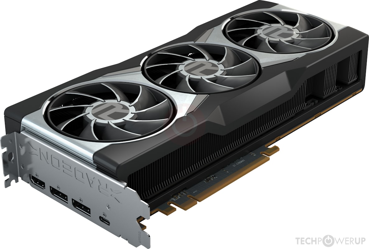
AMD gave RDNA 2.0 one last send off in 2021 with the Radeon RX 6950 XT, released for $1099. It was the same Navi 21 silicon as the RX 6900 XT, just tuned up with higher clock speeds and more power to go along with them. It didn't change the state of the GPU market, but it gave AMD a new flagship to wave around until the next generation arrived.
| Model | Codename | Architecture | Transistor Count | Video Memory | PCI-E Interface | TDP | Passmark Score |
| Radeon RX 6950 XT | Navi 21 XTX | 7nm RDNA 2.0 | 26.8 Billion | 16GB GDDR6 | PCI-E 4.0 | 335 Watts | ~28000 |
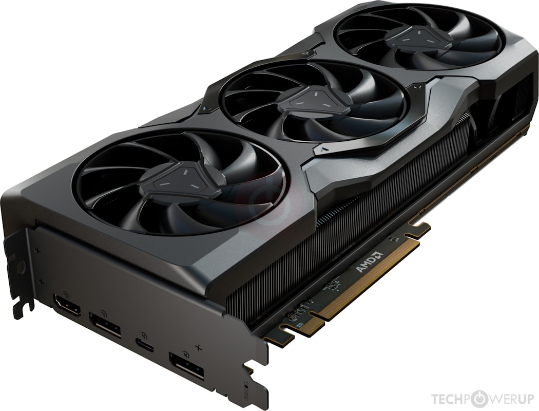
2022 brought the biggest architectural change to AMD GPUs since RDNA itself, when RDNA 3.0 introduced the first chiplet design on a consumer graphics card. Instead of one giant piece of silicon, the GPU was split into a single Graphics Compute Die made on TSMC's 5nm process, surrounded by a ring of smaller Memory Cache Dies made on 6nm. This let AMD build a massive GPU with a transistor count of 57.7 Billion without it becoming impossibly expensive to manufacture. The Radeon RX 7900 XTX released in December 2022 for $999 and went straight for the RTX 4080, while the RX 7900 XT released the same month for $899 with 20GB of VRAM to the XTX's 24GB. RDNA 3.0 also brought second generation Ray Accelerators, brand new AI Accelerators, support for DisplayPort 2.1, and hardware AV1 encoding, along with FSR 2.0 and 3.0.
| Model | Codename | Architecture | Transistor Count | Video Memory | PCI-E Interface | TDP | Passmark Score |
| Radeon RX 7900 XTX | Navi 31 XTX | 5nm/6nm RDNA 3.0 | 57.7 Billion | 24GB GDDR6 | PCI-E 4.0 | 355 Watts | 31438 |
| Radeon RX 7900 XT | Navi 31 XT | 5nm/6nm RDNA 3.0 | 57.7 Billion | 20GB GDDR6 | PCI-E 4.0 | 315 Watts | 29073 |
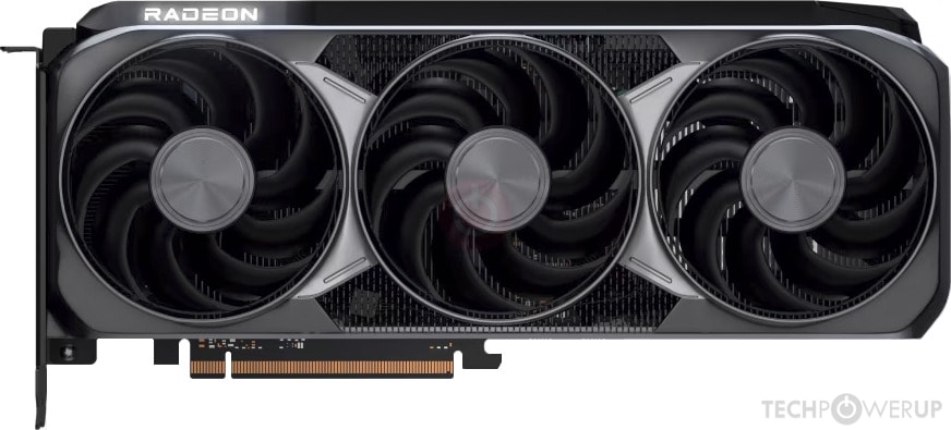
After sitting out 2023 and 2024, AMD came back in 2025 with RDNA 4.0. The Radeon RX 9070 XT released in March 2025 for $599. AMD made a bold move this generation and stopped trying to compete for the very top of the performance charts, instead focusing on making the best value cards it could. The 9070 XT went straight for Nvidia's mid range and came away with the win. RDNA 4.0's third generation Ray Accelerators doubled ray tracing performance per Compute Unit compared to RDNA 3, second generation AI Accelerators were added, and FSR 4 finally used machine learning for proper AI upscaling just like DLSS.
| Model | Codename | Architecture | Transistor Count | Video Memory | PCI-E Interface | TDP | Passmark Score |
| Radeon RX 9070 XT | Navi 48 XTX | 4nm RDNA 4.0 | 53.9 Billion | 16GB GDDR6 | PCI-E 5.0 | 304 Watts | 26924 |