
This is an overview of all modern Graphics Processing Units (GPU). Since there are so many we will split them up starting with Nvidia.
Birth of the Modern GPUThe modern GPU that we are familiar with today and the only kind of GPU that AMD, Intel, or Nvidia makes today is the kind with a Unified Shader architecture. A shader is how the computer calculates the lighting and color of an object simulated in a 3D scene. Before the unified shader paradigm, graphics cards would have separate dedicated hardware for each of the multiple steps of processing. The first step is Vertex Shading, calculating the lighting and color of the model of the object itself, the second step is the pixel shader where the color of each pixel on the computer's display is calculated. A Unified shader is a processor that is capable of calculating both of these steps rather than only just one.
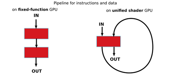
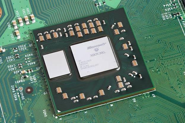
Using the separate shader hardware made the GPU less flexible and sometimes slower than intended if one set of processors was stressed more than the other set, leaving them idle and waiting for the other set. This led to the development of the Unified Shader processors, all-purpose processors that could handle all steps of the shader process. This made GPUs more easily expandable and more flexible, able to handle a wider array of tasks at the same time. The Unified Shader was first introduced in the Xbox 360 by ATI in November 2005, and then was quickly adopted by Nvidia for the desktop GPU lines. They even managed to beat ATI to market with this feature. Unified Shaders have been universally used on all desktop GPUs since then.
 Nvidia through the Generations
2006 - Tesla
Nvidia through the Generations
2006 - Tesla
Nvidia's first Unified Shader GPU was the GeForce 8800 GTX in November 2006 at $599. This GPU was built using a processor architecture that Nvidia called Tesla. This architecture introduced a great number of features that Nvidia still uses on their cards to this day, such as CUDA acceleration that allowed general purpose computing to happen on the GPU. Tesla was also Nvidia's first architecture to feature DirectX 10 support.
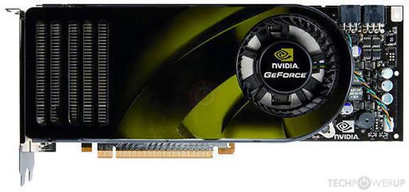
| Model | Codename | Architecture | Transistor Count | Video Memory | PCI-E Interface | TDP | Passmark Score |
| GeForce 8800 GTX | G80 | 90nm Tesla | 681 Million | 768MB GDDR3 | PCI-E 1.0 | 145 Watts | 657 |
2007 saw only a refined version of the 8800 GTX called the 8800 GT. Released in October 2007 for $249, it was the same Tesla architecture on a brand new 65nm process node. Along with some other cost saving improvements, it was able to match or closely follow the 8800 GTX for less than half the price. This is also where Nvidia made the switch to PCI-E 2.0.
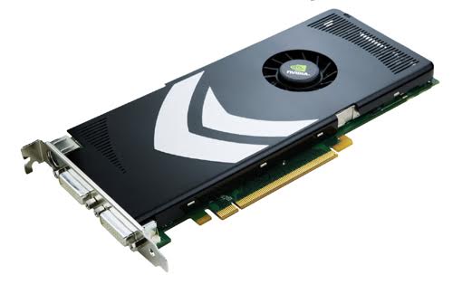
| Model | Codename | Architecture | Transistor Count | Video Memory | PCI-E Interface | TDP | Passmark Score |
| GeForce 8800 GT | G92 | 65nm Tesla | 754 Million | 1GB GDDR3 | PCI-E 2.0 | 125 Watts | 514 |
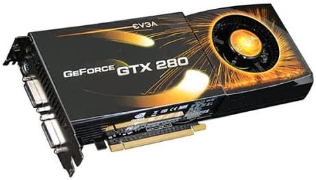
The next generation of Nvidia GPUs was a refined version of the same Tesla architecture using a 65nm process. The 9800 GTX released in April of 2008 for $350. 2008 sure was a wild year for Nvidia. Even though they had just launched the 9800 GTX, they introduced yet another flagship card with a new naming scheme just one month later! The GTX 280 was released June 2008 for $650. It used the same 65nm Tesla architecture as the 9800 GTX, but with a lot more transistors this time! Just one month after that, they followed up with the 9800 GTX+ that used a brand new 55nm process and double the VRAM in July 2008 for $229.
| Model | Codename | Architecture | Transistor Count | Video Memory | PCI-E Interface | TDP | Passmark Score |
| GeForce 9800 GTX | G92 | 65nm Tesla | 754 Million | 512MB GDDR3 | PCI-E 2.0 | 140 Watts | 769 |
| GeForce 9800 GTX+ | G92b | 55nm Tesla | 754 Million | 1GB GDDR3 | PCI-E 2.0 | 141 Watts | 746 |
| GeForce GTX 280 | GT200 | 65nm Tesla | 1.4 Billion | 1GB GDDR3 | PCI-E 2.0 | 236 Watts | 1040 |
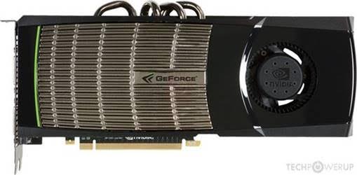
In 2010, Nvidia introduced a new architecture called Fermi with support for DirectX 11, starting with the GTX 480 in March 2010 for $499. The Fermi line is where Nvidia first started using the long-lived GDDR5 for the VRAM. Fermi was also infamously power hungry and ran very hot. So hot it required a huge metal housing that could reach an uncomfortable-to-touch 120 degrees F, and that is just the outside shroud around the heatsink! Later in November 2010, the GTX 580 was released for $499 as well! This card came with some bonus refinements like more VRAM and higher clock speeds, but most importantly lower power consumption and temperatures. Some of these improvements were achieved by clock throttling down when the card recognizes power use that is too high, in order to keep temperatures under control.
| Model | Codename | Architecture | Transistor Count | Video Memory | PCI-E Interface | TDP | Passmark Score |
| GeForce GTX 480 | GF100 | 40nm Fermi | 3 Billion | 1.5GB GDDR5 | PCI-E 2.0 | 250 Watts | 3595 |
| GeForce GTX 580 | GF110 | 40nm Fermi | 3 Billion | 4GB GDDR5 | PCI-E 2.0 | 244 Watts | 4617 |
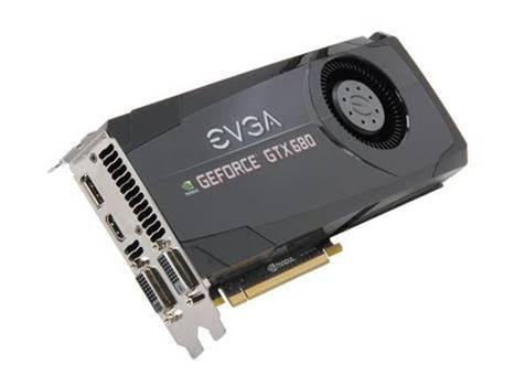
The GTX 680 was released in March 2012 for $500 using a new architecture called Kepler. Nvidia made the move to PCI-E 3.0 with this card. On the card itself were some big improvements, like a redesigned memory controller that pushed the GDDR5 memory even faster. So much faster that Nvidia could use a cheaper, smaller memory bus and still gain more performance. A hardware H.264 encoder was added that helped with capturing gameplay video and streaming gameplay over the Internet. G-sync also made its first appearance this year. Nvidia also did something very interesting this year. Previously the top tier GTX x80 flagship models were all Gx100 codename models. This year the GTX 680 is the smaller GK104. The Gx104 models had previously been the GTX x60 mid range cards…
| Model | Codename | Architecture | Transistor Count | Video Memory | PCI-E Interface | TDP | Passmark Score |
| GeForce GTX 680 | GK104 | 28nm Kepler | 3.5 Billion | 4GB GDDR5 | PCI-E 3.0 | 195 Watts | 5498 |
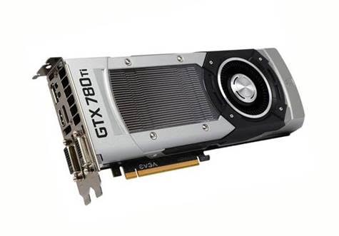
Nvidia took the opportunity to release BIG versions of Kepler this year, instead of the normal smaller and more refined versions. In February 2013, the GTX Titan appeared for $999, which was basically a huge version of the GTX 680 with a massive 6 GB VRAM. It was Nvidia saying that they own the pinnacle of single GPU gaming, graphics, and compute performance and they gave it a name to match. Another Big Kepler came again in May 2013 in the form of the GTX 780 for $499, and again in November 2013 in the form of the GTX 780 Ti for $699. Twice in one year, Nvidia created a new upper tier for the biggest, baddest GPU on the market with the Titan, and then the Ti models. That being said, they were all practically the same Big Kepler… But with differences in clock and memory speeds.
| Model | Codename | Architecture | Transistor Count | Video Memory | PCI-E Interface | TDP | Passmark Score |
| GeForce GTX Titan | GK110 | 28nm Kepler | 7 Billion | 6GB GDDR5 | PCI-E 3.0 | 230 Watts | 9064 |
| GeForce GTX 780 | GK110 | 28nm Kepler | 7 Billion | 3GB GDDR5 | PCI-E 3.0 | 230 Watts | 7900 |
| GeForce GTX 780 Ti | GK110 | 28nm Kepler | 7 Billion | 6GB GDDR5 | PCI-E 3.0 | 230 Watts | 9341 |
The next architecture introduced by Nvidia was the Maxwell architecture, but it wasn't immediately used for the next Generation of GPUs. First, Maxwell 1.0 was used in the lower end GTX 750 Ti (codenamed GM107) in February 2014. It can be considered a practice GPU for this new architecture, as it was the first time that a GPU included an on board ARM CPU of its very own. This allowed it to be more independent of the system's primary CPU, leaving more CPU resources for the games to take advantage of. A more refined version of the architecture called Maxwell 2.0 was introduced with the GTX 980 (codenamed GM204), which released in September 2014 for $549. A big improvement that Maxwell had over Kepler was power efficiency with the top end card, the GTX 980, being under 200 Watts!
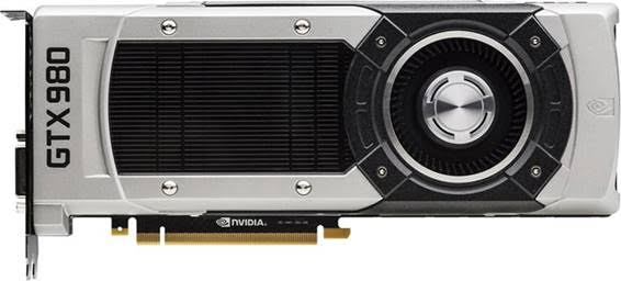
| Model | Codename | Architecture | Transistor Count | Video Memory | PCI-E Interface | TDP | Passmark Score |
| GeForce GTX 750 Ti | GM107 | 28nm Maxwell 1.0 | 1.8 Billion | 2GB GDDR5 | PCI-E 3.0 | 60 Watts | 3822 |
| GeForce GTX 980 | GM204 | 28nm Kepler | 5.2 Billion | 4GB GDDR5 | PCI-E 3.0 | 165 Watts | 10832 |
Nvidia continued the Titan line with its own Maxwell version, the Titan X, in March 2015 for the traditional $999. In June 2015, Nvidia released the GTX 980 Ti for $649.
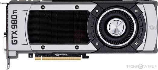
| Model | Codename | Architecture | Transistor Count | Video Memory | PCI-E Interface | TDP | Passmark Score |
| GeForce GTX Titan X | GM200 | 28nm Maxwell 2.0 | 8 Billion | 12GB GDDR5 | PCI-E 3.0 | 250 Watts | 12642 |
| GeForce GTX 980 Ti | GM200 | 28nm Maxwell 2.0 | 8 Billion | 6GB GDDR5 | PCI-E 3.0 | 250 Watts | 13702 |
A new architecture came to us in the form of Pascal, with the GTX 1080 having released in May 2016 for $599, along with the traditional Titan version named the Titan X again in August 2016 for $1200 this time. But don't worry, the 2015 version was named the GTX Titan X. This time it is just the Titan X. No confusion here… Pascal kept the very power efficient legacy of Maxwell, and introduced the new refined version of GDDR5 called GDDR5X, which allowed even higher memory clock speed. Along with some VR focused features, Pascal also focused on compute performance to help sales in the data-center and supercomputer markets.
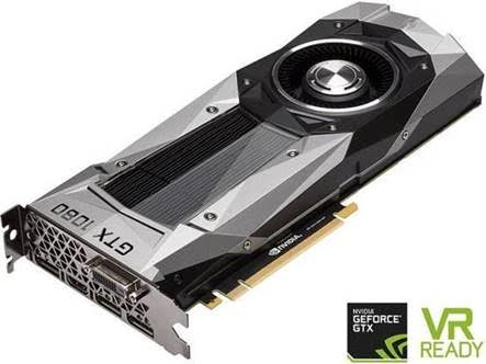
| Model | Codename | Architecture | Transistor Count | Video Memory | PCI-E Interface | TDP | Passmark Score |
| GeForce GTX 1080 | GP104 | 16nm Pascal | 7.2 Billion | 8GB GDDR5X | PCI-E 3.0 | 180 Watts | 14559 |
| GeForce GTX Titan X | GP102 | 16nm Pascal | 12 Billion | 12GB GDDR5X | PCI-E 3.0 | 250 Watts | 13659 |
In 2017, both the GTX 1080 and the Titan X got an upgrade. The GeForce GTX 1080 Ti released in March 2017 for $699. Then Nvidia seemed to suddenly realize that the Titan X product naming might be a bit confusing, so they made a new separate Titan. The GeForce Titan Xp released in April 2017 for $1200. A new architecture made a brief appearance this year as well. The Volta architecture appeared in the form of the GeForce Titan V in December 2017 for $2999. It only appeared in Titan cards, and was focused almost exclusively on datacenter compute and supercomputer usage. It also happened to use the new HBM2 memory. It seemed to be a practice card for testing new features and new memory types.
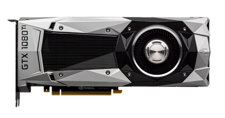
| Model | Codename | Architecture | Transistor Count | Video Memory | PCI-E Interface | TDP | Passmark Score |
| GeForce GTX 1080 Ti | GP102 | 16nm Pascal | 12 Billion | 11GB GDDR5X | PCI-E 3.0 | 250 Watts | 17349 |
| GeForce GTX Titan Xp | GP102 | 16nm Pascal | 12 Billion | 12GB GDDR5X | PCI-E 3.0 | 250 Watts | 16634 |
| GeForce GTX Titan V | GV100 | 12nm Volta | 21.1 Billion | 12GB HBM2 | PCI-E 3.0 | 250 Watts | 17883 |
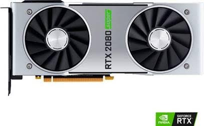
2018 brought a new architecture called Turing with some radical changes including a new naming scheme, the brand new GDDR6 memory, and what Nvidia hoped would be a killer feature. Nvidia introduced the RT processing cores and claimed that they were finally ready to perform real-time ray-tracing lighting in games! They were so excited about this feature that they changed the traditional GTX prefix to RTX, even though this was very close to the Radeon prefix of RX! The RTX 2080 launched in September 2018 for $799. Breaking tradition yet again, the RTX 2080 Ti was also released in September 2018 for $1199. The Titan RTX was released in December 2018 for $2499.
| Model | Codename | Architecture | Transistor Count | Video Memory | PCI-E Interface | TDP | Passmark Score |
| GeForce RTX 2080 Ti | TU102-300A | 12nm Turing | 18.6 Billion | 11GB GDDR6 | PCI-E 3.0 | 250 Watts | 21425 |
| NVIDIA Titan RTX | TU102-400 | 12nm Turing | 18.6 Billion | 24GB GDDR6 | PCI-E 3.0 | 280 Watts | 19849 |
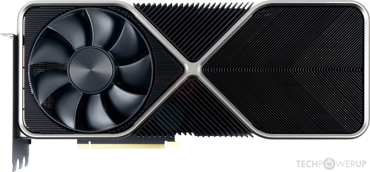
In 2020, Nvidia brought a brand new architecture called Ampere. The RTX 3080 launched in September 2020 for $699, followed just a week later by the RTX 3090 for $1499. Ampere was built on Samsung's 8nm process, and it introduced the brand new GDDR6X memory, at least for the highest end cards. The RT Cores were upgraded to their second generation and the Tensor cores to their third, which finally made DLSS actually worth turning on. DLSS 2.0 rendered the game at a lower resolution and used the Tensor cores to upscale it to full resolution in real time, giving a huge performance boost for almost no visible loss in quality. Ampere also brought the move up to PCI-E 4.0. Nvidia called the RTX 3090 the first 8K gaming GPU, and at $1499 it had better be able to do something impressive. Of course all that performance came with a cost, and Ampere gained a reputation for being almost as power hungry as Fermi back in 2010.
| Model | Codename | Architecture | Transistor Count | Video Memory | PCI-E Interface | TDP | Passmark Score |
| GeForce RTX 3080 | GA102-200 | 8nm Ampere | 28.3 Billion | 10GB GDDR6X | PCI-E 4.0 | 320 Watts | 24996 |
| GeForce RTX 3090 | GA102-300 | 8nm Ampere | 28.3 Billion | 24GB GDDR6X | PCI-E 4.0 | 350 Watts | 26511 |
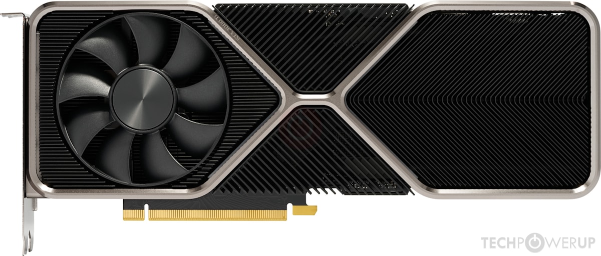
2021 brought a refreshed version of Ampere in the form of the RTX 3080 Ti, released in June 2021 for $1199. It was basically an RTX 3090 that had been cut down a little to slot in between the 3080 and the 3090 in both price and performance. It was a fantastic card, but the timing was terrible. 2021 was the middle of the great graphics card shortage, when crypto miners and scalpers were snatching up every card they could find, and actually getting one at a reasonable price felt like winning the lottery.
| Model | Codename | Architecture | Transistor Count | Video Memory | PCI-E Interface | TDP | Passmark Score |
| GeForce RTX 3080 Ti | GA102-225 | 8nm Ampere | 28.3 Billion | 12GB GDDR6X | PCI-E 4.0 | 350 Watts | 26750 |
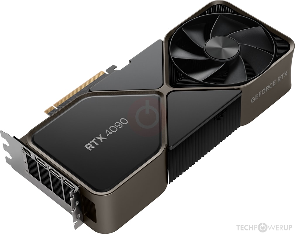
2022 started with one final Ampere flagship, the RTX 3090 Ti, released in March 2022 for $1999. It was the biggest, baddest, most power hungry version of Ampere that Nvidia ever made, demanding a massive 450 Watts. Later that year came a brand new architecture called Ada Lovelace. The RTX 4090 launched in October 2022 for $1599, and it was an absolute monster of a card. Built on TSMC's 4nm process, it was such a huge jump over Ampere that it felt like more than a single generation of improvement. Ada brought third generation RT Cores and fourth generation Tensor cores, along with a new feature called Shader Execution Reordering, a fancy name for hardware that sorts the work of the shader processors so they don't waste time sitting idle. Ada also introduced DLSS 3, which added AI generated frames on top of the AI upscaling. The RTX 4080 followed a month later in November 2022 for $1199, still a very powerful card even if it had to live in the shadow of the 4090.
| Model | Codename | Architecture | Transistor Count | Video Memory | PCI-E Interface | TDP | Passmark Score |
| GeForce RTX 3090 Ti | GA102-350 | 8nm Ampere | 28.3 Billion | 24GB GDDR6X | PCI-E 4.0 | 450 Watts | 29893 |
| GeForce RTX 4090 | AD102-300 | 4nm Ada Lovelace | 76.3 Billion | 24GB GDDR6X | PCI-E 4.0 | 450 Watts | 38041 |
| GeForce RTX 4080 | AD103-300 | 4nm Ada Lovelace | 45.9 Billion | 16GB GDDR6X | PCI-E 4.0 | 320 Watts | 34431 |
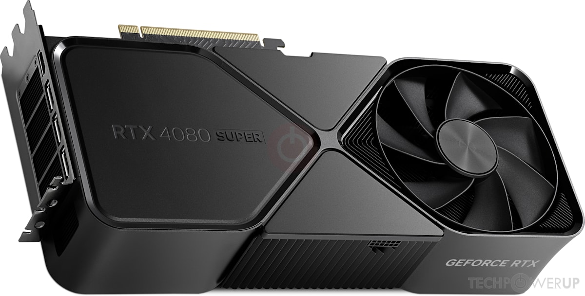
In January 2024, Nvidia brought back the SUPER name, which hadn't been seen since the 2010s, for a mid generation refresh of Ada Lovelace. The RTX 4070 Ti SUPER launched on January 24th for $799 and the RTX 4080 SUPER followed on January 31st for $999. Both cards were refinements of existing Ada designs with a few more cores switched on, and the 4070 Ti SUPER finally got a proper 16GB of VRAM. It wasn't the most exciting release in Nvidia's history, but it was a welcome return to cards that could actually be bought at their intended price.
| Model | Codename | Architecture | Transistor Count | Video Memory | PCI-E Interface | TDP | Passmark Score |
| GeForce RTX 4080 SUPER | AD103-400 | 4nm Ada Lovelace | 45.9 Billion | 16GB GDDR6X | PCI-E 4.0 | 320 Watts | 34228 |
| GeForce RTX 4070 Ti SUPER | AD103-275 | 4nm Ada Lovelace | 45.9 Billion | 16GB GDDR6X | PCI-E 4.0 | 285 Watts | 31831 |
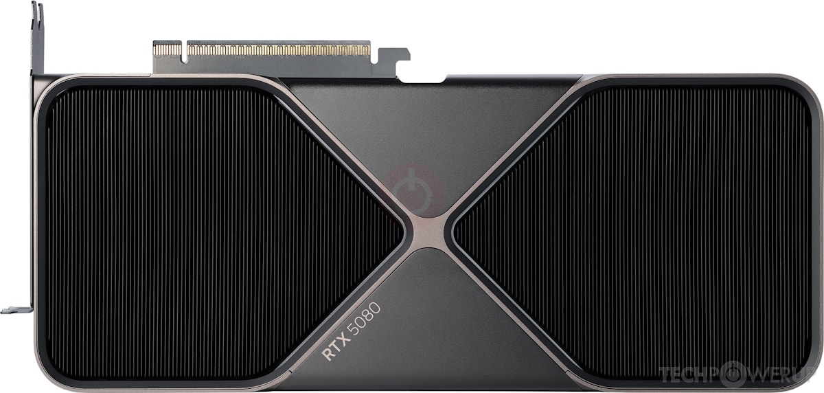
2025 brought yet another new architecture called Blackwell. The RTX 5090 launched in January 2025 for $1999, the most expensive flagship Nvidia had ever released. It was also the most powerful, and easily the most power hungry, with a TDP of 575 Watts. Blackwell used the brand new GDDR7 memory and moved up to PCI-E 5.0. The fifth generation Tensor cores added support for FP4 precision, and DLSS 4 introduced Multi Frame Generation, which uses AI to generate multiple new frames for every single frame the GPU actually renders. It was a ridiculous card, in almost every sense of the word.
| Model | Codename | Architecture | Transistor Count | Video Memory | PCI-E Interface | TDP | Passmark Score |
| GeForce RTX 5090 | GB202-300 | 4NP Blackwell | 92.2 Billion | 32GB GDDR7 | PCI-E 5.0 | 575 Watts | 38962 |